产品说明
一般描述
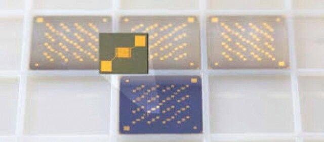
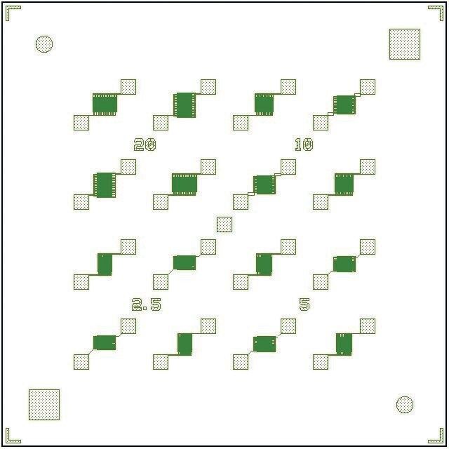
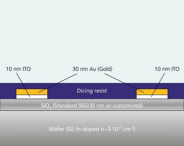
Substrate: 150 mm wafer according to semiconductor standard (used for bottom-gate)
Layer structure:
应用
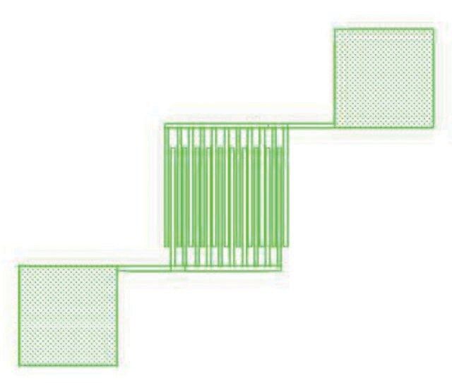
Back-gated OFET Interdigitated Substrate (organic field-effect transistor) can be used in the fabrication of chemical sensors for potential usage in pH sensing and detection of immunoassays. It can also be used in the fabrication of biosensors by coating the sheets of the FET with a specific antibody for the detection of SARS-CoV-2. FET based biosensors can be potentially used in clinical diagnosis, point of care testing, and on-site detection.
包装
diced wafer on foil with air tight packaging
制备说明
Recommendation for resist removal:
To guarantee a complete cleaning of the wafer / chip surface from resist residuals, please rinse by acetone and then dry the material immediately by nitrogen (compressed air).
Recommendation for material characterization:
If gate currents appear during the characterization of the field effect transistors, considerable variations could occur at the extraction of the carrier mobility. Therefore it is necessary to check the leakage currents over the reverse side (over the chip edges) of the OFET-substrates.
储存及稳定性
Store the wafers at a cool and dark place and protect them against sun.
Resist layer was applied to prevent damage from scratches.
Expiration date is the recommended period for resist removal only. After resist removal, the substrate remains functional and does not expire.
法律信息
Product of Fraunhofer IPMS
产品性质
| 形式 | chips (diced) |
| 包装 | pack of 1 (wafer of 60 diced chips) |
| 储存温度 | 15-25℃ |
 m.cnreagent.com